Mike's SCARA Robot

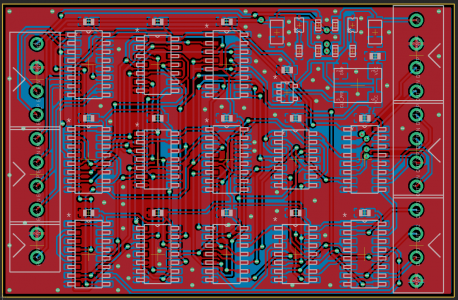
Board is routed!

I gave it a good go trying to do it by hand, but kept getting myself stuck. Ran the autorouter and was able to find a solution that worked well. I spent some extra time cleaning up the traces it left with sharp corners or weird squiggly lines. I added a ton of GND vias to stitch the planes together.

The board passes a design rule check with 10 thou traces and 10 thou spacing.

I still need to do the following:
  • Finish stitching the GND planes
  • Verify the schematic one more time
  • Quadruple check the terminal block spacing (I want them to snap together)
  • Manually add device labels and silk screen text.
1592314167822.png

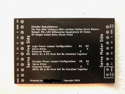
A couple of features that I added last minute were two blue LEDS. One to indicate logic power and one for encoder power. Additionally, I included solder jumper pads to select between the logic being powered by the servo drive or the external power supply, and a second set for the encoder.

For my robot, I cannot power the encoder from the drive, but if anyone ever wanted to run just a single motor connected to a drive, then the drive power supply could be used by changing the jumper on the board.

100uF ceramic caps filter both power supplies, and a larger buffer package was added because I had space. Every chip is decoupled by a 0.1uF ceramic cap.

I opted for no mounting holes at this time to keep the size down. It will hang in-line with the encoder cable, probably just below the drive.
 
I used a profile that I found from someone else and probably some online documentation. While I don't know for sure, I think that the main purpose of the heating profile is to
1. Allow all the parts to come up to temp at the same time even with different thermal characteristics
2. To be above the reflow temp for the shortest period of time.

So basically pre-heat everything evenly to just below reflow, then bring above reflow and cool down.

In the end for me, this worked so I avoided trying to fix what was not broke :). If I was in production (Electronics is just another hobby) I would spend more time to optimize.
There are two reasons for the stepped-temperature profile. One is to drive any absorbed water off in a fairly gentle manner so the SMD's (and board) don't delaminate due to the so-called popcorn effect -- absobed water turns into steam inside the packages or layers and expands the molding compound or board enough to break bond wires or board vias. Seen it. It can cause really baffling failure modes. The other issue is that the flux in solder paste has a certain amount of water in it, so if it's heated too fast it literally bubbles up and can move parts around before the solder melts. Seen that, too, but it is more of an issue with very small parts -- CSP's in particular (and you _probably_ aren't using any of those).

Toaster ovens are cheap so a nice solution for hobbyists that assemble boards on an occasional basis. Way cheaper than an SMD rework station.
 
Boards have been ordered! Have to place the order for all the components too and pick up some solder paste. I got 25 boards (added $2 over getting 5) and a stencil for $16 + shipping. I hope the quality is good!

Even more, I hope the circuit is correct. It all works in my head, but we will have to wait and see if all of those electrons go where they are supposed to.

On the side, my plan is to work with @ats1911 and @brino to develop a CPLD solution to this problem. It seems way over my head, but the parts are cheap and supposedly are perfect for what I am trying to do! I'm excited to learn about them.
 
Mike, from what we have seen here, you and your buddy are more than capable of designing your own VHDL/Verilog source code, committing them to parts and building what ever complex circuits you want!

This should be a fun project for all of us!

-brino
 
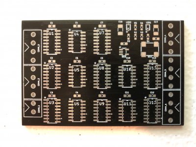
The demultiplexer boards are here! I have assembled a test article and plan on testing it this weekend. I'm going to hold off on assembling them all until I am sure that they work as intended.

I ordered them from JLCPCB with black solder mask and Hot Air Solder Leveling. For how inexpensive these were, I am very impressed by the quality.

image010.jpg

image011_LI.jpg

Before assembling the board, I did a 100% test of every connection against the original schematic by doing a point to point check with a multimeter. This hopefully would have caught any errors in either my PCB routing or the manufacturer. Everything looked great!

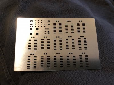
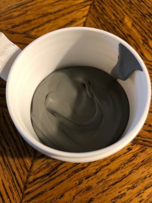
For those unfamiliar, this board uses surface mount components which are typically soldered with solder paste (a sludge of atomized solder and flux). The paste is placed only on the pads that need solder by use of a laser cut stencil (additional $9 to my order).

image009.jpg

image008.jpg

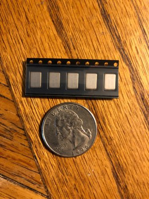
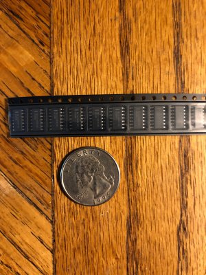
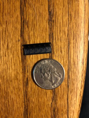
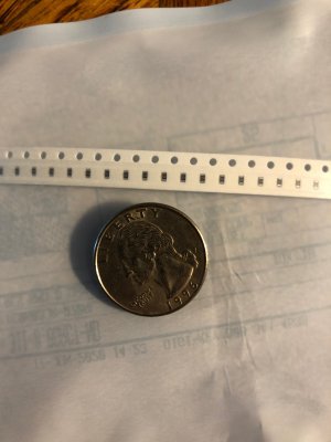
Once the paste is applied to the pads, you can use tweezers to place the components. Finally a specialized heat gun is used to reflow the solder paste and make the electrical connections. This worked almost perfectly and I bet I can even better with some practice. Here are some components for size reference.

Crystal oscillators:
image001.jpg

14-SOIC package integrated circuits (this board uses a mix of 14 and 16 pin chips in SOIC packaging):
image003.jpg

SOT-23/5 Digital Buffers:
image006.jpg

0603 (60 thou by 30 thou) size resistors and capacitors:
image007.jpg

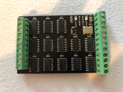
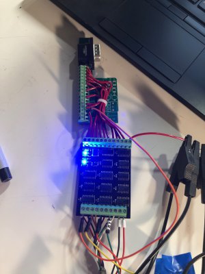
And here is the board all assembled. The encoder input signals come in from the left and snake their way through all the integrated circuits. The encoder outputs to the drive (with commutation and index signals) exit on the right. At the top right, you can see the power filtering, LED indicators, clock source, and jumpers.

image012.jpg

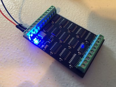
The logic powers up perfectly. If I were to do this again, I would probably pick a larger resistor value for the LED. It is very bright.

image015.jpg

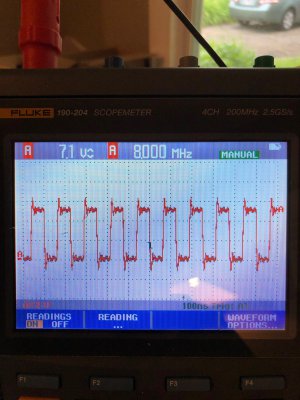
Using the oscilloscope, I was easily able to pick up the 8MHz clock signal (the squiggles are mostly from the length of socpe probe wire)

image016.jpg

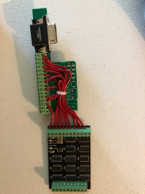
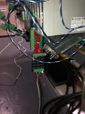
Here is my adapter board hooked up to the Allen Bradley servo drive breakout board. It just hangs beneath. I might machine or 3D print a case.

image017.jpg

And finally, mounted to the servo drives.

image018.jpg

I plan on powering this up today and scoping all the input and output signals. I am maybe 60% confident that it will work correctly and produce the desired outputs. There is a big question of how the drive will handle the initial power on of the encoder. No halls signals can be generated until the motor has moved at least 3 counts (sometimes 4). I still think the encoder might do something funny at power on to setup the halls outputs, but we will have to see. Worst case, I'll have to manually push the robot around just a little bit before it can be run by the servo drives.

I'll get more pics of the soldering process when I do the next 4 boards.

-Mike

EDIT: A bit more learning about PCBs after this order was placed would drive me to make the following changes on a second revision if one were ever made:
  • Fusing on the input to protect the drive or external power supply
  • Reverse polarity protection on power inputs
  • Footprints to prevent the possibility of adding two jumpers at the same time on the input power configuration (could damage drive)
  • ESD protection diodes on all pins
  • Footprints for optional LEDs on all input and output pins (easier troubleshooting)
  • Extend the board and add Silkscreen for the terminal connections to the top of the board
  • Mounting holes
  • Fix the LED footprints (they were wrong from an online download and were quite difficult to solder.
  • Change the encoder side terminal blocks from 10 to 12 and include a place to land a cable shield and pass it through to the drive
 
Last edited:
Mike,

The boards look great, congratulations!

Your list of improvements looks like a list of our DFx guidelines from work (DFM=Design For Manufacture, DFT=Design For Test, etc.)

The only (small) piece of advice I could add would be to add some "rework" room between the outside rows of logic devices and the connectors. If you find that you need to add one jumper to one of those device pins you'll have a hard time getting a soldering iron in there to do it.

This project continues to impress!

-brino

Thanks for the tip and the compliments! I am guessing I'll make a slightly modified revision B of this board and I'll try to add some more room! If you had any other general DFM tips and tricks, I'd love to know more about them. Pretty new to the whole PCB world.
 
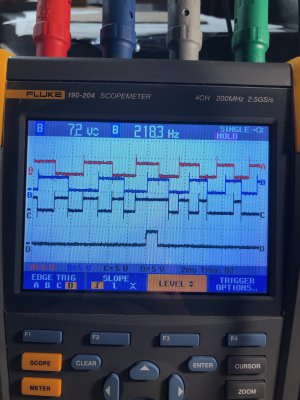
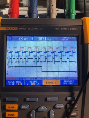
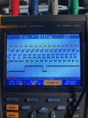
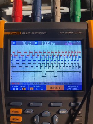
Started testing the board on the robot. I began by hooking the board up to the encoder but not plugging it into the drive. I used the oscilloscope to measure the input A, B, & C channels while using the 4th probe to test various points on the board. This would be an excellent for a Mixed Signal Oscilloscope with a logic analyzer (lots of digital only channels), but I don't have one. Here's what I found.

61489870910__8B78F863-59EF-4267-AC40-7B9A960715D0.JPG

The A, A*, B, & B* signals all come through very cleanly and the output voltage is right on the money. Since these more or less pass through the board, they don't have any distortion or glitches. As a bonus, the use of the transceivers on the board clean up the noise spikes that come from the robot wiring before it hits the drive.

The Z index signal turns on and off at the right time - once per revolution - and rises and falls sharply. It is ON for 1 quadrature count. Unfortunately there are a lot of little glitches in the signal. They seem to be (I haven't fully tested this yet) a one clock cycle high pulse when the signal should be low. The bottom trace (D) is the Z index signal and the lower middle trace (C) is the multiplexed signal from the encoder. The three high counts in a row on the C trace triggers the output of the pulse on D.

61489872260__B9775E47-48ED-4EA7-90D0-D04CE1963712.JPG

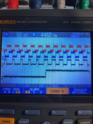
The S1, S2, and S3 signals properly decode the encoded C channel. Each of the signals rise and fall at the correct transition between patterns on the C channel. I am so stoked about this. There is really no reason why this couldn't have completely failed to work at all, but somehow I was actually able to learn enough about digital circuits to build a board that decoded them! Here are some pictures showing the transition of one of the hall effect commutation signals at the transition of a pattern on the C channel.

IMG_9220.jpg

IMG_9221.jpg

Just like the Z channel, there are extremely brief pulses (either high or low) that are not supposed to occur. More concerning however are glitches that turn OFF the output for exactly 3 counts when it should be ON.

IMG_9222.jpg

IMG_9224.jpg

My working theory is that both types of glitches occur at the rising and falling edges of the signals and happen when the clock pulse occurs at a bad time. For example, lets say A is HIGH and B is rising, and at the same time C is falling. At this exact moment, the clock samples the input. It registers A and B as HIGH but C had not yet fallen low enough and gets sampled HIGH. This passes the incorrect information into the circuit and a different pattern is detected and the output glitches high or low. On the next clock pulse, the input is sampled again and the error is corrected, giving a 1 clock pulse glitch on the output.

The worse case is when the sample occurs on the falling edge of a quadrature count. Lets use the same example as before A is HIGH, B is rising and C is falling. This time the clock pulse arrives a few nanoseconds earlier and the inputs are sampled. A is sampled as HIGH, B has not risen high enough so it is sampled as LOW, and C has fallen low enough to be sampled as LOW. In this case the state we are exiting (A high B low) is sampled incorrectly and a glitch is passed into the circuit. Unfortunately on the next clock pulse, B has risen HIGH and we are in a new state (A high B high). The erroneous sample is latched into memory until 3 quadrature counts have occurred and the first state (A high B low) is presented again and is sampled correctly. I think that this is what is occurring in the pictures above.

I'm probably going to ask for advice on the electronics forum that I joined during this project. I don't think normal noise suppression techniques will help the short glitches because the signal is being driven by a powerful transceiver rather than weak radiated emissions and it definitely won't help the larger glitches. I think this is just an issue with trying to sample a parallel asynchronous signal (encoder input) into a synchronous clocked circuit.

More to follow...
 
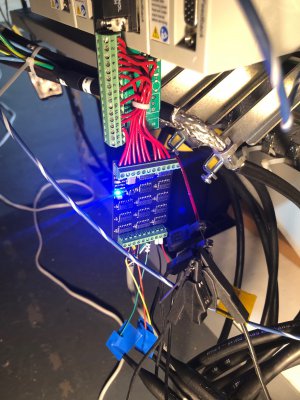
After testing the circuit on the bench, I hooked it up to the servo drive, edited the CMF file to indicate the motor has hall effect commutation signals, and download the configuration to the PLC.

The mess of wires all over the place are the scope probes for testing. The wiring is pretty clean with just the encoder.

IMG_9216.jpg

The drives accepted the configuration and were immediately able to read the A and B feedback channels (the motor position updated correctly when I turned the motor shaft by hand). In the motor configuration menu is a page called "Hookup". These Hookup Tests are the most important thing to tell you if the drive and motor are configured and wired properly.

The first test is called the "Marker Test". It requires you to rotate the motor shaft by hand and the test will complete when the marker/index/Z pulse is found. This should always occur in the same position. When I ran this test, it would complete in random locations within a quarter turn of the shaft. I'm pretty sure the drive is picking up the 1 clock cycle (125 ns) glitches and thinking they are the marker pulse. This means that without correcting my adapter board, I will not be able to home to the index pulse on the motor. This doesn't prevent me from running the motor thankfully.

The second test is called the "Feedback Test" and it requires you to define a distance and rotate the shaft manually. When the correct distance has been reached, the test completes and the feedback polarity is set in software. This tests the correct quadrature counts are being received by the drive. I was able to complete this test without issue.

The final test is the most important and is called the "Command and Feedback Test". The drive powers the motor open loop and monitors the position and commutation feedback. This test passes when the motor moves the correct distance as specified in the test setup and the drive detects no wiring errors. This test will fail if the motor power wires are swapped (UVW) or the commutation signals are swapped (S1, S2, & S3).

This test gave me the most trouble because the Yaskawa motors are wound differently than AB motors and therefore use a different convention for the assignment of U, V, & W and S1, S2, & S3. There are 36 possible combinations of these signals and it took me 12 different combinations before I found one that passed the hookup test (took me 2 hours). I want to finish testing the rest of the combinations because I expect to find 2 more valid combinations.

Once the hookup test was passed I immediately moved on to the Autotune. This powers the motor with a high open-loop torque and uses the measured response to find the system dynamics. From this information, the drive calculates appropriate gains for the servo loop to give good response. This test completed properly, however testing at higher speeds generated failed tests and a couple of motor overspeed faults on the drive. These should never happen and indicate something could be wrong with the commutation still.

Finally, with the motor sorta tuned, I tried to issue commands to the motor. It energized and held position properly and I was able to command indexing moves with acceleration and deceleration. I did notice that after some period of time the moves would fail and the motor would begin vibrating uncontrollably. Additionally I felt "soft" spots in the motors rotation where I could easily overpower the motor by hand. All of this tells me I am very close but the commutation still isn't perfect.

I have three theories on this one. #1 is that while I passed the hookup test, the motor power wiring and hall effect commutation signals are still not correct. That's why I wanted to test the 24 remaining wiring configurations. #2 is that the glitches in the commutation signals create regions of poor control in the motor. I don't think that this is really the case though because the "soft" spots in the motor are much larger than the 3 counts that the glitches seem to appear for. I can hear these glitches are audible popping of the motor shaft as it rotates however. #3 is that my circuit is not decoding the commutation signals properly. I don't have any evidence for this, but it is a possibility. All the scope traces look like it is doing everything properly, however I need to do much more comprehensive testing to really rule this one out. Probably the best test would be to scope the signal into the ASIC on the encoder again and compare it to the output of my PCB. They should be identical.

I'm feeling like I'm in the home stretch of getting this working.

Here is a short video of the motor executing indexing moves.

View attachment IMG_9228.MOV
 
Last edited:
That’s some amazing work and progress. I’m rooting for ultimate success and impressed with what you have done so far. I’ve made a couple PCBs, a couple including some degree of SMDs. But nothing as detailed as what you are doing. I love it.
 
Back
Top