Needing more than a spark test?

I decided to design a PCB for my pocketgeiger-to-Teensy signal-conditioning circuit. Mostly as a way to learn how to use EasyEDA. When I was using ExpressPCB I got kind of spoiled by having 4 layer PCB's available for not a lot of money so, although it's overkill, I went with a 4-layer PCB for this one. It really does make it easier to lay out boards if you can avoid all the Vcc/Vee/Gnd traces by just sinking a via down to a power or ground plane. Even with the two "extra" layers, it only cost $7 for five boards (the minimum quantity they will make). That includes silk screen and solder mask layers for the top and bottom! It cost more for the shipping than to make the darn boards! The SMT components I don't already have are on order from Mouser

Anyway, I've attached the schematic to show folks what I'm up to. There should be enough comments there to figure things out, but if not I'd be happy to clarify. I'm using the LMC662 because it should have very low current noise (Iin = 2FA @RT). The input RC time constant is 10 seconds so it won't distort the low-speed signal coming out of the pocketgeiger board. It's important to minimize baseline drift because that will affect the peak voltage, which is what the MCA uses to determine what element(s) are present.
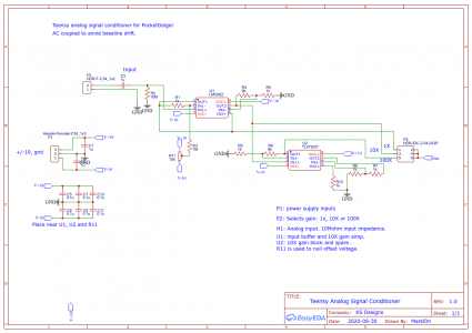
Schematic_teensy ADC signal conditioner_2020-09-05_14-04-51.png
 
You have been busy!
Have you simulated this one?
I have been otherwise occupied. I have to get back into this.

My first thought about PCB layout involving 4 layers (yes - I have gone to 6 layers at times), is the design philosophy about shielding, and having the circuits in between copper planes for Vcc, Gnd, etc. When it comes to dealing with noise, a ground (or power) plane is not just a place where the operating currents from any device can simply be dumped into. I found that by putting carefully placed slots into the ground/power planes, one can "guide" the current paths so as to prevent any more energetic device from polluting the signal in an input circuit via common mode return impedances. I am thinking you probably already know this.

I will get to understand it better soon. My first reaction is that I see a 1978 device, and a 1998 device, both of which I have used extensively - back in the 1990's. :) That's OK. For this purpose, a JFET Op-Amp is perfectly fine, and comes in packages with pins that make it "constuctable" without needing fancy PCB assembly kit. For me , a 1uF cap with a 10M resistor as a simple 1-pole low pass filter with a 10 seconds time constant up front is confusing.

Baseline drift is solved by clamping, and DC coupled goodness. Alternatively, zero drift switched AC circuits. Earlier in the thread, I spoke of finding just the right amount of front end gain, while also going for getting some power into it (lower impedance more robust signal). A follower at the front (LMC662) with a 1K feedback resistor only does the latter. The buffer stage gain is only 1 - or else I misunderstand.

To get a signal up and away from noise, the very first device it finds must have a very low noise figure, and importantly, must have enough gain to amplify the signal (and the noise) to such a level that any subsequent circuit contributions to noise cease to be significant.

Have you simulated this design?
 
Last edited:
Mark - remind me where we get the
I decided to design a PCB for my pocketgeiger-to-Teensy signal-conditioning circuit.
Mark - just to catch me up on this. There are things I am not understanding.

From your post #306, you found the (quite expensive) X100-7 photodiode array, and a Hackaday posting which described direct detection of gamma rays, and describes relative insensitivity to gamma energy in pulse height, but that there was information in the pulse width. OK - so we don't know why there was energy storage in the diode that only delivers late, but we think measuring the pulse width, possibly then multiplied by a height value, could make it useful?

In the same post - there is reference to the Instructables schematic which you did not like because it looked like it had a unbiased AD743 BiFET Op-Amp with a 1pF hanging on it. You may be right, and I am skipping along too fast here to give it the full attention, but the first swift look at the data sheet shows a spectacularly low noise very high performance amplifier which would surely show the door to a LMC662. Agreed, we may not like the circuit it got put in, or it's lack of bias, but I do like the data sheet as a starting point.

Moving on (to catch up). You found the SparkFun module SEN-14209 at $69.95 from DigiKey which apparently incorporates the X100-7 sensor.
Is this one of those "economies of scale" things where a £100.05 sensor can arrive on a $69.95 built module?

So what I get from this is that the GeigerCounterType5_circuit_diagram is what is on the module, and you (rightly) don't like it, and so you make your own PCB, and use the X100-7 (at $69.95). Did I get that right?

While I am going to mess with the PMT - even if only as a comparative cross-check, (let each test the other), I propose to sync up and go with the sensor you are using. I just needed to be sure that I am not making a mistake here.

Which vendor did you use? I think I may have to set up with Digi-Key. Mouser has a whole bunch of dev boards, but not, apparently, that one. :confused:
 

Attachments

  • AD743.pdf
    290.5 KB · Views: 1
  • GeigerCounterType5_circuit_diagram.pdf
    60.8 KB · Views: 1
You have been busy!
Have you simulated this one?
I have been otherwise occupied. I have to get back into this.

My first thought about PCB layout involving 4 layers (yes - I have gone to 6 layers at times), is the design philosophy about shielding, and having the circuits in between copper planes for Vcc, Gnd, etc. When it comes to dealing with noise, a ground (or power) plane is not just a place where the operating currents from any device can simply be dumped into. I found that by putting carefully placed slots into the ground/power planes, one can "guide" the current paths so as to prevent any more energetic device from polluting the signal in an input circuit via common mode return impedances. I am thinking you probably already know this.

I will get to understand it better soon. My first reaction is that I see a 1978 device, and a 1998 device, both of which I have used extensively - back in the 1990's. :) That's OK. For this purpose, a JFET Op-Amp is perfectly fine, and comes in packages with pins that make it "constuctable" without needing fancy PCB assembly kit. Forme , a 1uF cap with a 10M resistor as a simple 1-pole low pass filter with a 10 seconds time constant up front is confusing.

Baseline drift is solved by clamping, and DC coupled goodness. Alternatively, zero drift switched AC circuits. Earlier in the thread, I spoke of finding just the right amount of front end gain, while also going for getting some power into it (lower impedance more robust signal). A follower at the front (LMC662) with a 1K feedback resistor only does the latter. The buffer stage gain is only 1 - or else I misunderstand.

To get a signal up and away from noise, the very first device it finds must have a very low noise figure, and importantly, must have enough gain to amplify the signal (and the noise) to such a level that any subsequent circuit contributions to noise cease to be significant.

Have you simulated this design?
No, I haven't simulated the design. As far as choice of opamp goes, just about anything that has internal compensation and compatible footprint could be used. I put the LMC662 and TL072 in there mostly because I have them on hand (and the LMC662 is used in the PocketGeiger). They are SOIC style packages so not too difficult to hand-solder.


I've done some RF PCBs, to the extent of making some test structures to check the impedance of asymmetrical strip lines. But for this low-speed circuit I was more interested in ease of layout (along with minimizing noise).
 
Mark - remind me where we get the

Mark - just to catch me up on this. There are things I am not understanding.

From your post #306, you found the (quite expensive) X100-7 photodiode array, and a Hackaday posting which described direct detection of gamma rays, and describes relative insensitivity to gamma energy in pulse height, but that there was information in the pulse width. OK - so we don't know why there was energy storage in the diode that only delivers late, but we think measuring the pulse width, possibly then multiplied by a height value, could make it useful?

In the same post - there is reference to the Instructables schematic which you did not like because it looked like it had a unbiased AD743 BiFET Op-Amp with a 1pF hanging on it. You may be right, and I am skipping along too fast here to give it the full attention, but the first swift look at the data sheet shows a spectacularly low noise very high performance amplifier which would surely show the door to a LMC662. Agreed, we may not like the circuit it got put in, or it's lack of bias, but I do like the data sheet as a starting point.

Moving on (to catch up). You found the SparkFun module SEN-14209 at $69.95 from DigiKey which apparently incorporates the X100-7 sensor.
Is this one of those "economies of scale" things where a £100.05 sensor can arrive on a $69.95 built module?

So what I get from this is that the GeigerCounterType5_circuit_diagram is what is on the module, and you (rightly) don't like it, and so you make your own PCB, and use the X100-7 (at $69.95). Did I get that right?

While I am going to mess with the PMT - even if only as a comparative cross-check, (let each test the other), I propose to sync up and go with the sensor you are using. I just needed to be sure that I am not making a mistake here.

Which vendor did you use? I think I may have to set up with Digi-Key. Mouser has a whole bunch of dev boards, but not, apparently, that one. :confused:
I bought the module directly from SparkFun. I've purchased stuff from them before and like supporting them. It isn't their design, though. It looks like it was designed as a response to the radiation released from Japanese reactors that were damaged by the tsunami. The relatively low price, compared to the expensive-by-itself detector, is a bit of a head-scratcher, so you could be right about the economies of scale.

So, on to the module itself. I have been planning on leaving the detector on the board, and tapping into the analog signal coming out of the second LMC662. The module is convenient because it has an on-board 27V bias generator for the detector. The analog signal, along with the detector bias voltage, is brought out to some pads on the back side of the board (probably to facilitate board testing). I HAVE simulated the analog portion of the module, but only so far as to get some sense of the pulse height/width coming out of the front end -- and use the data to test some peak-finding methods.

Since the X100-7 is in a DFN style package it should be possible to extract it from the board and repurpose it, but for a first crack at an XRF system I just want to know if there's even the ghost of a chance it will work for us. If I DID take the repurposing route I'd put the detector on its own separate board so I could easily test different circuit designs. As you have pointed out, the AD743 bests the LMC662 on a number of specs. And there are a number of auto-zeroing amplifiers one could use to boost the signal level so there's no doubt there is room for improvement -- if preliminary results justify it.

The design I was critical of is a completely different one that was an electrical engineering student's class project.
 
OK - your reply happened while I was typing.

Firstly - if you want a custom proto circuit, before one thinks about taking the chip off the board, there is probably more mileage in modifying the board, and/or, removing some components, and mounting it straight on top of board of your own. A bit hack, but I don't like de-soldering small pin semiconductors, especially those which cost more than 10 bucks for one!
- - - - - - - - -
Re: Noise
The trouble with noise is, even if it is in a low speed circuit, the noise it adds can be full spectrum. If the interface cable goes to PC, or Arduino, or something, unless the PC audio innards are designed to have returns isolated from the digital electronics, like the best motherboards featuring onboard audio do, an instrumentation signal can get drowned. We need not be too concerned about noise if we get the S/N ratio preserved on a signal large enough, and low impedance enough, to make it immune, so that it could be casually taken via an audio cable to a PC. Better still, get it into numbers before it goes to the display device - via USB.

I may be getting a little too over-critical on this. It comes from the days when I had to crawl through a DC4, preserving a 15uV signal from a bridge sensor that was at the rudder, through a maze 400Hz inverter high current cables making exceptional splat. I found out about balanced differential pairs, and double screening with the inner connected at only one end, and how it was possible to collect even tiny currents if you controlled what other currents could be added to them, or induced in them.
- - - - - - - - -
I may end up with my own flavour [OK - flavor], of input data sample collect circuit , but that's OK. I am still motivated to make it go using the ready-made board. That is - unless you think a de-solder and fit to one of your boards is easy enough. I guess I don't like de-solder reworks, even using the Polish coil-wire trick to take them off unharmed.

The Op-Amp pin format was, and is, a remarkable casual "standard". "Other" Op-Amp circuits we contrive may well be built on the module board.
Unlike the more usual situation where manufacturers try to invent their own standards, with the aim of making their kit compatible only with their own, on this feature, if they could not offer "plug-in" replacements or upgrades, they were doomed.

I also get it that components with part designations beginning with "AD" can have a price premium, and it goes crazy if they have "883D anywhere else in the code.

Regarding the kind of pulse response, and the Hackaday article about (pulse height x duration) being important, I think there is no problem in integration the pulse energy in software. I do think that getting at more than one pulse in ten seconds is something we should go for.
So - ordering one for me sometime tonight.

[Edit - new distraction - how much old Mercedes estate car stuff one has to fight through to get at a screen-wash pump]! :confused 3:
 
With the right tools it's not too difficult to remove most SMT parts from boards. A temp-controlled hot plate can do it, if you're careful. Lead-free solder melts at a higher temp than 60/40 so the hot plate needs to get up to 300C or thereabouts. Before de-soldering, you must bake the board @80C for a couple of hours to remove moisture, otherwise the water could turn into steam and "popcorn" your part, breaking bond wires.

After removal, the package pins need to be re-tinned, mostly to re-level them. You need to do that in order to mount them on another PCB.

BTW, when creating footprints for QFN or DFN style parts, it's really handy to include a silk screen outline of the package. This makes it easier to align the package w/respect to the soldering points of the footprint. If you've had to roll your own footprints, you probably know that anyway, but I thought it was worth mentioning.
Yep - you and I seem to have traveled the same road.
I had some solder+flux paste stuff in a pack with a tiny needle that would temporarily "stick" the little 0402 components down "sort of" in place, then I relied on the silkscreen boundaries and surface tension to let them "flow" into place. They kind of centre up by themselves, except the odd one now and then that would go into tombstone attitude. That company had a real nice regulated hotplate that could be programmed to do a "cook" sequence. There was also an IR thing that could take a board up to heat, and hold it for just the right number of seconds. All that is now in a past life. :)

Making one's own footprints, especially those for microwave RF, that have loads of parallel shunt inductance grounding vias, was a tedious business! That's not even counting the simulations to get at the S-parameters. For home stuff, most times I can go for the luxury of packages I can work with. Even SO8 seems "big" these days. I am not even beyond using stuff with through-hole pins 0.3" apart, on 0.1" pitch if it's something useful that I happen to have around.

I think the point of all those "hats" and add-on development boards that fit on Raspberry Pi('s) GPIO pins. It's to let us us folks with real fingers, and schoolkids, be able to work with them.

The SparkFun website crapped out on me repeatedly, even when trying using two FireFox browsers, and one Chromium-based "Brave" browser. The site works, but kept going into a pointless loop near the end when trying to pay up. The folk at SparkFun emailed me. I'm going to have another go at it, maybe tomorrow.
 
It's odd you ran into problems trying to buy stuff at SparkFun, but it sounds like they're trying to take care of you.

Regarding the self-align effect with SMTs, it works the same with pre-tinned pins and pads -- as long as you have some solder flux in there, too. Of course, solder paste has flux in it so no problem there. A few times we did have alignment problems when the water in the flux started to boil off. On occasion the part would move around too much to get the self-align to work -- but if you were alert you could nudge the part back into position before the solder actually melted. It was cool to see the part suddenly move over a bit as the surface tension did its thing.

The solder paste method is the way to go if you are soldering multiple parts at the same time. Our test boards typically had just one IC package on them so our simpleminded approach worked fine.. The remaining components were hand-soldered.
 
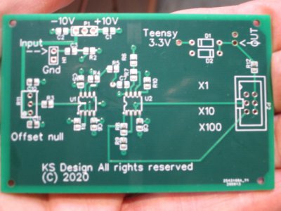
The PCBs arrived today. They look pretty good, and ohmed out OK so at least I know I didn't screw up when I placed the vias. Here's a photo of the unpopulated board:

MCA signal conditioner.JPG

The board differs a little from the schematic I showed in an earlier post. I added some clamp diodes and a limiting resistor to ensure the signal going into the Teensy doesn't go below ground or above the Teensy's supply voltage. I don't want to damage my $20 controller board!

The "KS Design" name is taken from our street name. I've used it for a few other PCBs as well, but no commercial stuff yet.

The board is much bigger than it really needed to be, and 4 layers are overkill for a design like this. The back side of the board only has a few traces on it. But it does make for a much cleaner layout. Anyway, $7 for five of them isn't going to break the bank. I can't believe how cheap PCBs are these days! Years back when I was designing and building audio gear it was much more expensive (for just 2 layers and no through-hole plating), plus it was necessary to lay the boards out on Mylar using tape and stick-on pads. Sooo much easier now.
 
Last edited:
Back
Top